
The Field Programmable Gate Array (FPGA) is a special mass-produced integrated circuit “chip” that consists of an array of thousands of “logic cells” interconnected by a dense matrix of wire segments and electronic switches. Those switches are selectively turned on by the device “program” to make connections between wire segments in the matrix and to the terminals of the logic cells to create a digital logic circuit with the logic cells as the components and the wires and switches in the wiring matrix used as the wires between the components.
The screen capture below is from the Xilinx FPGA editor tool showing the structure of a small portion of the array. The darker blue boxes are collections of logic cells (called configurable logic blocks by Xilinx). The local wiring segments are grey, while longer wire segments are depicted in magenta. The wire segments used in this design are highlighted in cyan, as are connections within the switch matrices. The switch matrices are recognized by the jumble of wires adjacent to each pair of configurable logic blocks. The pattern shown here is repeated throughout the device. Notice the logic cells are small compared to the area taken up by the switches and wiring. While the depiction is not to scale, the fact is the silicon area occupied by the wiring matrix and switches is far larger than the area occupied by the logic cells: there is a lot of overhead to make the “wiring” programmable.
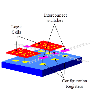 1 Conceptual FPGA showing configuration layer below circuit layer
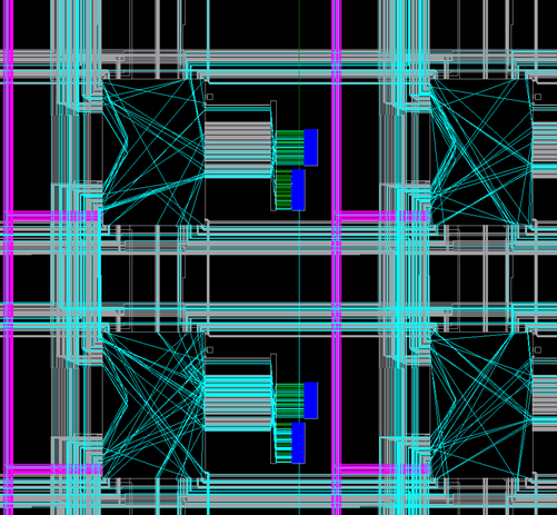 A small section of the FPGA showing routing and configurable logic blocks (blue)
In contrast to custom logic devices, the function of these devices is determined by a user configuration program rather than during the device manufacture; they are programmed after the devices are fielded, hence the moniker “field programmable gate array”. Depending on the device, the program is either “burned” permanently or semi-permanently into the device as part of the product manufacture, or is loaded into the device from an external memory every time the device is powered up. Allowing the user to determine the function permits economies of scale in the chip manufacture and gives the user access to complex integrated designs without the high non-recurring engineering costs associated with application specific integrated circuits.