Distributed arithmetic is a bit level rearrangement of a multiply accumulate to hide the multiplications. It is a powerful technique for reducing the size of a parallel hardware multiply-accumulate that is well suited to FPGA designs. It can also be extended to other sum functions such as complex multiplies, fourier transforms and so on. Look at my Radar on a chip paper for an application example of distributed arithmetic.
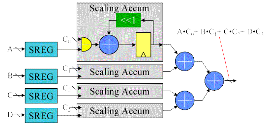
In most of the multiply accumulate applications in signal processing, one of the multiplicands for each product is a constant. Usually each multiplication uses a different constant. Using our most compact multiplier, the scaling accumulator, we can construct a multiple product term parallel multiply-accumulate function in a relatively small space if we are willing to accept a serial input. In this case, we feed four parallel scaling accumulators with unique serialized data. Each multiplies that data by a possibly unique constant, and the resulting products are summed in an adder tree as shown below.
If we stop to consider that the scaling accumulator multiplier is really just a sum of vectors, then it becomes obvious that we can rearrange the circuit. Here, the adder tree combines the 1 bit partial products before they are accumulated by the scaling accumulator. All we have done is rearranged the order in which the 1xN partial products are summed. Now instead of individually accumulating each partial product and then summing the results, we postpone the accumulate function until after we’ve summed all the 1xN partials at a particular bit time. This simple rearrangement of the order of the adds has effectively replaced N multiplies followed by an N input add with a series of N input adds followed by a multiply. This arithmetic manipulation directly eliminates N-1 Adders in an N product term multiply-accumulate function. For larger numbers of product terms, the savings becomes significant.
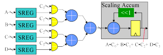
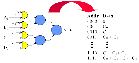
Further hardware savings are available when the coefficients Cn are constants. If that is true, then the adder tree shown above becomes a boolean logic function of the 4 serial inputs. The combined 1xN products and adder tree is reduced to a four input look up table. The sixteen entries in the table are sums of the constant coefficients for all the possible serial input combinations. The table is made wide enough to accommodate the largest sum without overflow. Negative table values are sign extended to the width of the table, and the input to the scaling accumulator should be sign extended to maintain negative sums.
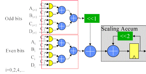
Obviously the serial inputs limit the performance of such a circuit. As with most hardware applications, we can obtain more performance by using more hardware. In this case, more than one bit sum can be computed at a time by duplicating the LUT and adder tree as shown here. The second bit computed will have a different weight than the first, so some shifting is required before the bit sums are combined. In this 2 bit at a time implementation, the odd bits are fed to one LUT and adder tree, while the even bits are simultaneously fed to an identical tree. The odd bit partials are left shifted to properly weight the result and added to the even partials before accumulating the aggregate. Since two bits are taken at a time, the scaling accumulator has to shift the feedback by 2 places.
This paralleling scheme can be extended to compute more than two bits at a time. In the extreme case, all input bits can be computed in parallel and then combined in a shifting adder tree. No scaling accumulator is needed in this case, since the output from the adder tree is the entire sum of products. This fully parallel implementation has a data rate that matches the serial clock, which can be greater than 100 MS/S in today's FPGAs.
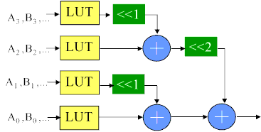
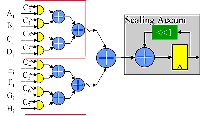
Most often, we have more than 4 product terms to accumulate. Increasing the size of the LUT might look attractive until you consider that the LUT size grows exponentially. Considering the construction of the logic we stuffed into the LUT, it becomes obvious that we can combine the results from the LUTs in an adder tree. The area of the circuit grows by roughly 2n-1 using adder trees to expand it rather than the 2n growth experienced by increasing LUT size. For FPGAs, the most efficient use of the logic occurs when we use the natural LUT size (usually a 4-LUT, although and 8-LUT would make sense if we were using an 8 input block RAM) for the LUTs and then add the outputs of the LUTs together in an adder tree, as shown below.